- 您现在的位置:买卖IC网 > Sheet目录3862 > PIC16F916-I/ML (Microchip Technology)IC PIC MCU FLASH 8KX14 28QFN
201
8018P–AVR–08/10
ATmega169P
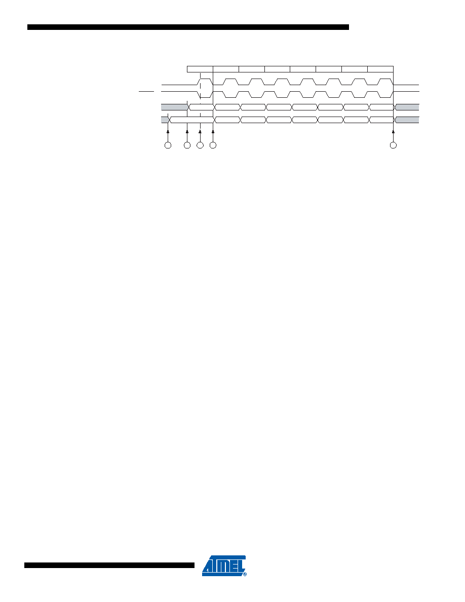
Figure 20-3. Three-wire Mode, Timing Diagram
The Three-wire mode timing is shown in Figure 20-3 At the top of the figure is a USCK cycle ref-
erence. One bit is shifted into the USI Shift Register (USIDR) for each of these cycles. The
USCK timing is shown for both external clock modes. In External Clock mode 0 (USICS0 = 0), DI
is sampled at positive edges, and DO is changed (Data Register is shifted by one) at negative
edges. External Clock mode 1 (USICS0 = 1) uses the opposite edges versus mode 0, that is,
samples data at negative and changes the output at positive edges. The USI clock modes corre-
sponds to the SPI data mode 0 and 1.
Referring to the timing diagram (Figure 20-3), a bus transfer involves the following steps:
1.
The Slave device and Master device sets up its data output and, depending on the proto-
col used, enables its output driver (mark A and B). The output is set up by writing the
data to be transmitted to the Serial Data Register. Enabling of the output is done by set-
ting the corresponding bit in the port Data Direction Register. Note that point A and B
does not have any specific order, but both must be at least one half USCK cycle before
point C where the data is sampled. This must be done to ensure that the data setup
requirement is satisfied. The 4-bit counter is reset to zero.
2.
The Master generates a clock pulse by software toggling the USCK line twice (C and D).
The bit value on the slave and master’s data input (DI) pin is sampled by the USI on the
first edge (C), and the data output is changed on the opposite edge (D). The 4-bit counter
will count both edges.
3.
Step 2. is repeated eight times for a complete register (byte) transfer.
4.
After eight clock pulses (that is, 16 clock edges) the counter will overflow and indicate
that the transfer is completed. The data bytes transferred must now be processed before
a new transfer can be initiated. The overflow interrupt will wake up the processor if it is
set to Idle mode. Depending of the protocol used the slave device can now set its output
to high impedance.
20.2.2
SPI Master Operation Example
The following code demonstrates how to use the USI module as a SPI Master:
SPITransfer:
sts
USIDR,r16
ldi
r16,(1<<USIOIF)
sts
USISR,r16
ldi
r16,(1<<USIWM0)|(1<<USICS1)|(1<<USICLK)|(1<<USITC)
SPITransfer_loop:
sts
USICR,r16
lds
r16, USISR
sbrs
r16, USIOIF
MSB
654321
LSB
1
2
3
4
5
6
7
8
654321
LSB
USCK
DO
DI
D
C
B
A
E
CYCLE ( Reference )
发布紧急采购,3分钟左右您将得到回复。
相关PDF资料
PIC16C716-20I/P
IC MCU OTP 2KX14 A/D PWM 18DIP
PIC18F26K80-I/SO
MCU PIC 64KB FLASH 28SOIC
PIC18F26J13-I/SS
IC PIC MCU 64KB FLASH 28SSOP
SFW27R-1STE1
SFW27R-1STE1-FFC/FPC CONN
PIC18F66J15-I/PT
IC PIC MCU FLASH 48KX16 64TQFP
PIC24FV32KA302-I/SO
MCU 32KB FLASH 2KB RAM 28-SOIC
PIC24HJ64GP204-I/ML
IC PIC MCU FLASH 64K 44-QFN
SFW27R-2STE1
SFW27R-2STE1-FFC/FPC CONN
相关代理商/技术参数
PIC16F916-I/SO
功能描述:8位微控制器 -MCU 14KB FL 352R 25 I/O RoHS:否 制造商:Silicon Labs 核心:8051 处理器系列:C8051F39x 数据总线宽度:8 bit 最大时钟频率:50 MHz 程序存储器大小:16 KB 数据 RAM 大小:1 KB 片上 ADC:Yes 工作电源电压:1.8 V to 3.6 V 工作温度范围:- 40 C to + 105 C 封装 / 箱体:QFN-20 安装风格:SMD/SMT
PIC16F916-I/SO
制造商:Microchip Technology Inc 功能描述:8 Bit Microcontroller Clock Speed:20MHz
PIC16F916-I/SOG
制造商:Microchip Technology Inc 功能描述:8BIT MCU FLASH SMD 16F916 SOIC28
PIC16F916-I/SP
功能描述:8位微控制器 -MCU 14KB FL 352R 25 I/O RoHS:否 制造商:Silicon Labs 核心:8051 处理器系列:C8051F39x 数据总线宽度:8 bit 最大时钟频率:50 MHz 程序存储器大小:16 KB 数据 RAM 大小:1 KB 片上 ADC:Yes 工作电源电压:1.8 V to 3.6 V 工作温度范围:- 40 C to + 105 C 封装 / 箱体:QFN-20 安装风格:SMD/SMT
PIC16F916-I/SP
制造商:Microchip Technology Inc 功能描述:8 Bit Microcontroller Clock Speed:20MHz
PIC16F916-I/SS
功能描述:8位微控制器 -MCU 14KB FL 352R 25 I/O RoHS:否 制造商:Silicon Labs 核心:8051 处理器系列:C8051F39x 数据总线宽度:8 bit 最大时钟频率:50 MHz 程序存储器大小:16 KB 数据 RAM 大小:1 KB 片上 ADC:Yes 工作电源电压:1.8 V to 3.6 V 工作温度范围:- 40 C to + 105 C 封装 / 箱体:QFN-20 安装风格:SMD/SMT
PIC16F916-I/SS
制造商:Microchip Technology Inc 功能描述:8-Bit Microcontroller IC
PIC16F916T-E/MLC02
制造商:Microchip Technology Inc 功能描述: